Navigating the Essentials of Custom PCB Design for IoT Projects
In the realm of Internet of Things (IoT), where innovation meets connectivity, the design of Printed Circuit Boards (PCBs) plays a pivotal role. The intricacies and importance of custom PCB design for IoT projects are innevitable, as we embark on a journey through the heart of electronic ingenuity.
The Foundation: Custom PCBs Unleashed: At the core of any IoT device lies a meticulously crafted PCB. Unlike off-the-shelf solutions, custom PCBs are tailored to the specific requirements of your IoT project. This bespoke approach not only optimizes space but also enhances performance, a critical factor in the interconnected world of IoT.
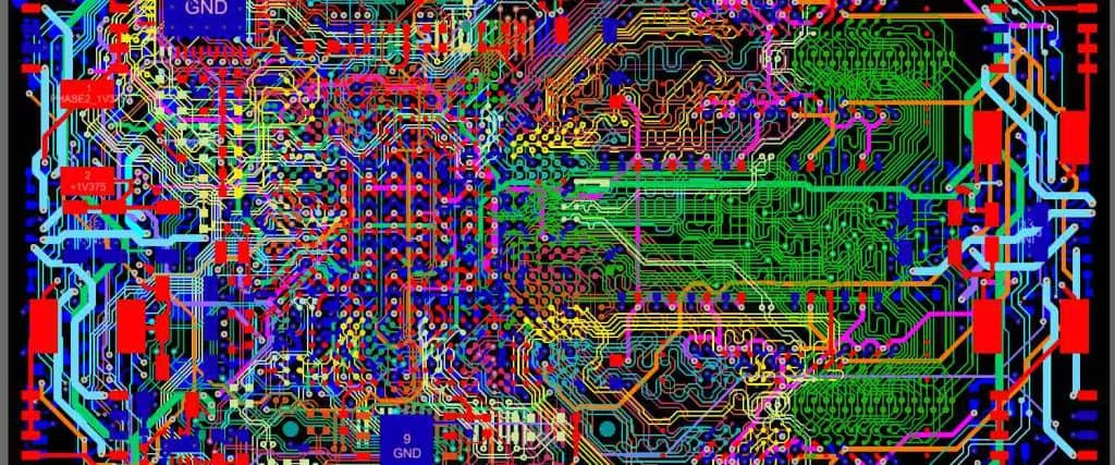
Size Matters: Miniaturization and Optimization: In the IoT universe, where real estate is a precious commodity, custom PCB design excels in the art of miniaturization. Through strategic component placement and routing, designers can shrink the size of the PCB without compromising functionality, a crucial aspect for IoT devices with size constraints.
Power Efficiency: The Dance of Components: Custom PCB design allows for the strategic placement of components to optimize power distribution and minimize energy loss. This dance of components ensures that IoT devices operate with maximum efficiency, a vital consideration in scenarios where battery life is a critical factor.
Tailored Connectivity: The IoT Web of Components: IoT devices thrive on connectivity, and custom PCBs weave the intricate web that connects sensors, processors, and communication modules. By tailoring the layout to the specific needs of your project, you can optimize signal integrity, reduce electromagnetic interference, and ensure seamless communication between components.
Component Selection: The Art of Choosing Wisely: In custom PCB design for IoT projects, every component matters. From microcontrollers and sensors to communication modules, the art lies in choosing components that align with your project’s requirements. Customization allows for the selection of components that strike the perfect balance between performance, cost, and power consumption.
Iterative Prototyping: Perfecting the Blueprint: The beauty of custom PCB design lies in its iterative nature. Prototyping becomes a playground for experimentation, refinement, and perfection. With each iteration, designers can fine-tune the layout, address potential issues, and ensure that the final PCB is a flawless manifestation of the IoT vision.
Considerations for Manufacturability: From Prototype to Production: As your IoT project transitions from prototype to production, manufacturability becomes a critical consideration. Custom PCB design allows for careful consideration of manufacturing constraints, ensuring that the design is not only functional but also feasible for mass production.

In the dynamic landscape of IoT, where innovation is the currency and connectivity the language, custom PCB design emerges as a silent hero. It’s the backbone that supports the intricacies of your IoT project, a canvas where creativity meets functionality. As you embark on your IoT journey, remember that the design of your PCB is not just a technical detail; it’s a blueprint for the future you’re about to create. In the world of IoT, where every connection matters, the design of your custom PCB is the wiring that shapes the future.
